Surface Microscopy with Cold Atoms

High-performance sensors provide insights that can hugely impact on all disciplines and on everyday life. Nowadays, the level of accuracy and precision achieved in controlling trapped cold quantum gases make these devices ideal sensors for detecting and studying new materials, geometries and devices.
In our "Microscopy Lab", we are building a surface microscope that probes local magnetic fields using Bose-Einstein condensates (BEC). The field sensitivity of an ultracold atom-based microscope is very high since the relevant energy scales in the gas are very low. When a Bose-Einstein condensate is used, quantum statistics cause accumulation of the atoms in the lowest possible energy state, thus effectively alleviating the complication of the gas’ temperature (the remaining dominating energy scale is the chemical potential, stemming from the residual interactions between the atoms). At such low energies, atoms then become extremely good sensors of their ambient magnetic field landscape.

Our custom-built UHV PCB for atom transportation.
The short animation below aims to illustrate this technique:
Surface Microscopy with Cold Atoms


Research and technology in this area is located at the interface between engineering, quantum theory and surface science. To substantially enhance the performance of BEC microscopes in terms of sensitivity, spatial resolution and dynamical range, the atom-surface distance should be reduced. Current atom chip technology allows trapping distances of a few micrometers, with further reduction typically becoming difficult due to distance-dependent effects such as Johnson noise, Casimir-Polder interactions, or stray fields, for example. We aim to bring atoms close to specially-engineered surfaces in which these effects are reduced, in order to achieve sub-micron trapping and thereby enable detailed studies, characterisation, and better understanding of atom-surface effects. In order to precisely position ultracold quantum samples in the vicinity of a variety of surfaces, we have developed a PCB for efficient, versatile transportation of atoms.

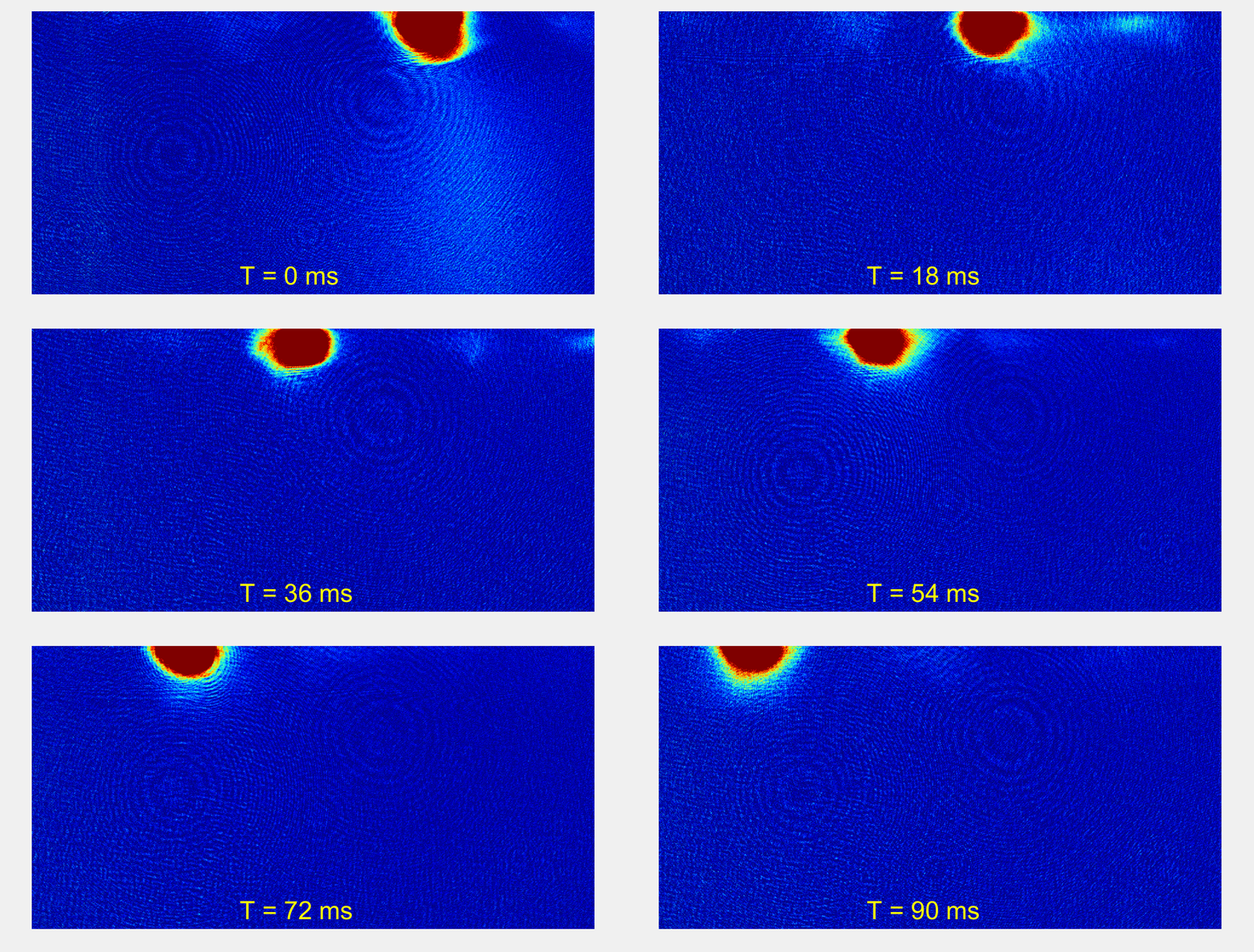
An atom cloud being transported over a distance of ~1cm towards the sample to be probed.
We aim to demonstrate the capabilities and practical use of the device by mapping surface patterns emerging in the submicron vicinity of new two-dimensional materials, such as graphene, and purpose-designed geometries, such as nano-structured (e.g. hyperbolic) metamaterials. Extension of BEC microscope to life science will play an important role across science and technology as it should allow probing the characteristics of organic, inorganic, and even living biological, materials.
For more information, or to join our team, don't hesitate to get in touch!
